In the first half of 2025, I, a masters 2nd year student, was fortunate enough to secure a profoundly enriching internship at HORIBA Instruments (Shanghai). My role during this internship at HORIBA was Opto-Electronic Engineer. HORIBA is leading global manufacturer of high-precision analytical instruments originating from Japan, is renowned worldwide for its excellence in spectroscopy and chromatography. My time there coincided with a major strategic evolution for the company in China—a concerted shift toward establishing integrated R&D and develop manufacturing capabilities right in the China local market.
This “Made In China, for China”initiative was not merely a business adjustment; it was a strategic pivot aimed at leveraging local engineering talent to develop world-class instruments, most notably the new Multifunction Optoelectronic Microscope designed in China, with a more competitive cost structure, all while maintaining HORIBA’s world-renowned standard of accuracy and precision.
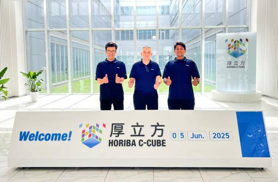
First day at Horiba Shanghai C-Cube
Upon joining HORIBA, I immediately became immersed in this significant strategic shift. The move symbolized the company’s dedication to accelerating product development cycles and controlling the entire supply chain, transitioning from an import-dependent operation to a self-sufficient powerhouse for instrument development. This new strategy meant that every design decision I made had direct implications for the future assembly line. The core goal of this initiative was to successfully launch a new local instrument that was fundamentally designed for efficient, high-quality local manufacturing—a distinction that provided the deepest practical learning experience of my internship.
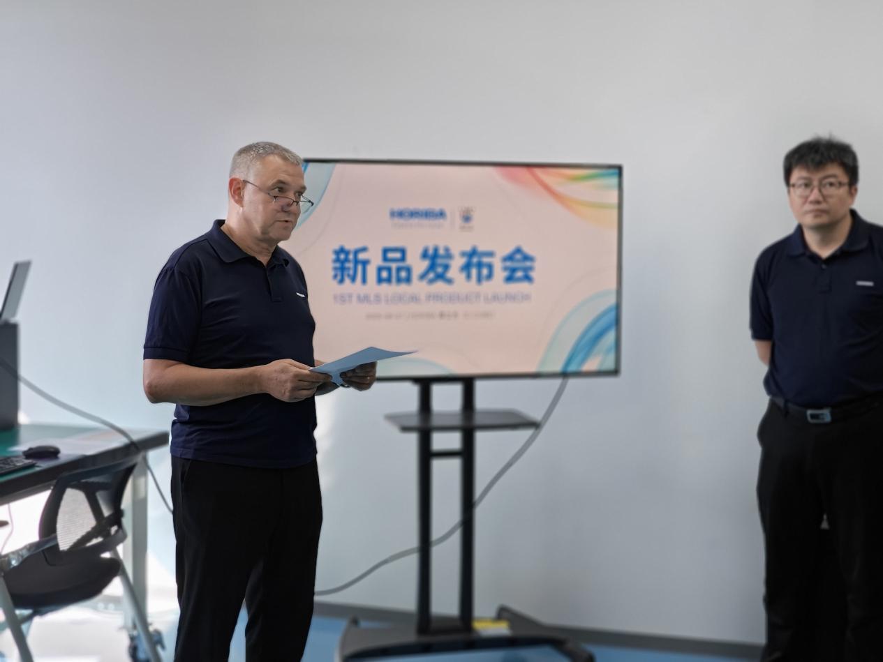
New Product Launch Event
As a member of the Material Life Science R&D team, my primary responsibilities were squarely focused on the system-level design and control integration for this new local instrument. Under the direct guidance of my manager, Mr. Franck Dhalenne, transfer from HORIBA France for mission in China, whose technical philosophy centered on merging robust optical design principles with agile development practices. I contributed to several critical technical areas, my work demanded a deep consideration of Design for Manufacturing (DFM) principles, moving beyond theoretical ideals to practical, cost-effective solutions. For instance, I was tasked with the mechanical design of key subsystems, utilizing Autodesk Fusion 360 to model components such as the Multifunction Optoelectronic Microscope laser holder, precision slider mechanism etc. I learned that true high-precision engineering is about ensuring long-term mechanical stability and alignment accuracy while simplifying assembly for the production floor.
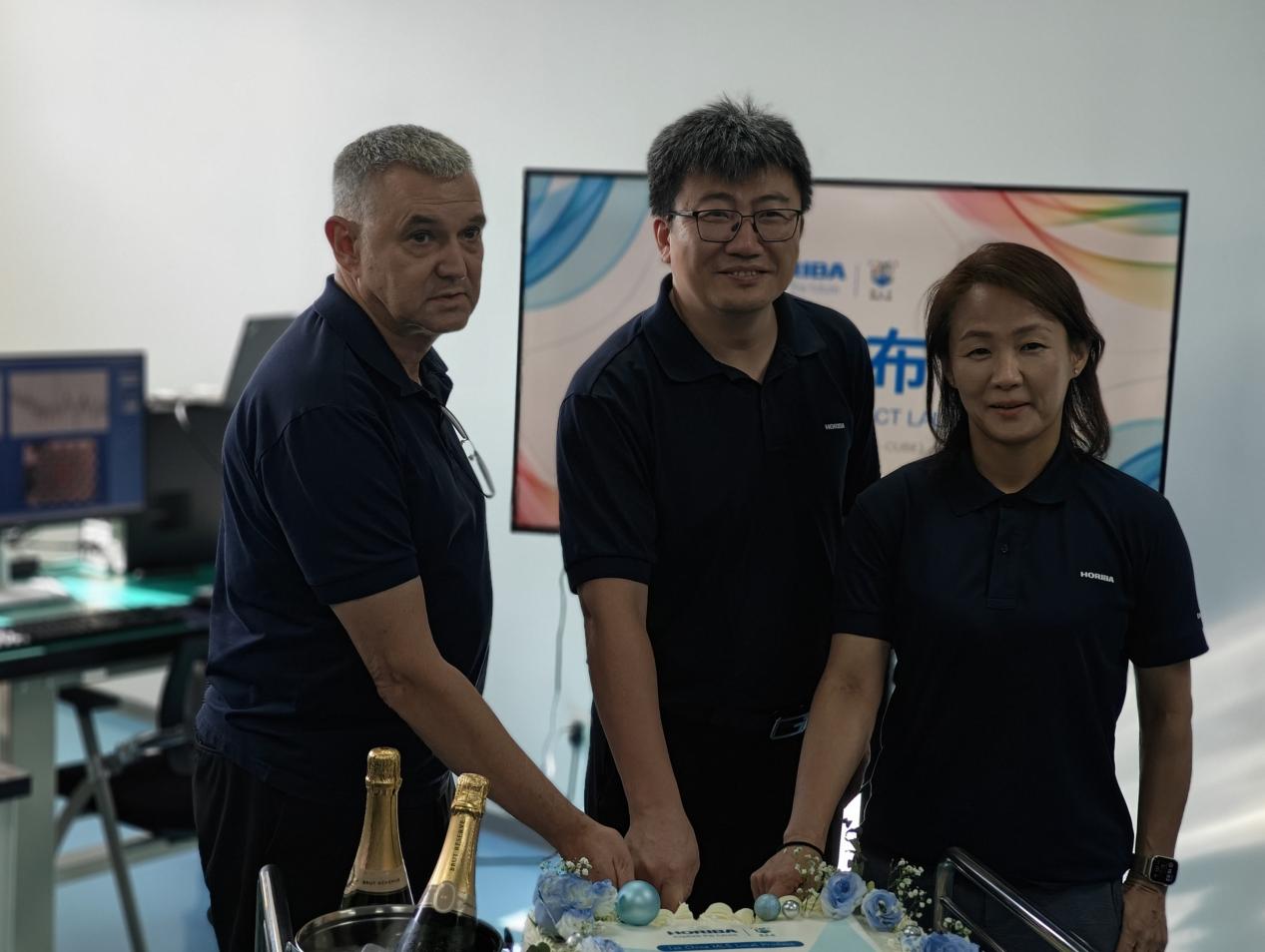
A Milestone Achieved: Celebrating the China-Manufactured Multifunctional Microscope
A crucial part of my technical contribution involved ensuring the instrument’s optical integrity, which directly impacts its final performance specifications. I participated in the vital optical calibration process, specifically for the selection and validation of band-pass filters, an area where spectral purity is paramount. This hands-on involvement taught me the rigorous quality control protocols and the fine-tuning required to achieve the necessary signal-to-noise ratio essential for a commercial-grade spectrometer. Furthermore, collaborating closely with CAE engineers, I contributed to the structural frame design, learning how to optimize a component’s weight and material usage while simultaneously maximizing its rigidity and vibrational damping—a critical factor for preserving spectral resolution once the instrument is operational in a lab or industrial setting.
My most significant learning curve, however, came from helping to transition the design from R&D prototyping to manufacturing readiness, bridging the gap between the lab bench and the factory . Furthermore, I focused heavily on the control system architecture, defining the precise communication protocol addresses and register configurations using Modbus RTU. This work effectively established the hardware-software interface, allowing for precise, automated command execution and reliable data acquisition, which is essential for both the automated quality control procedures during manufacturing and the final user experience.
My internship was defined by an environment that strongly emphasized both technical excellence and global teamwork. I was surrounded by a diverse, multinational team—a key characteristic of a global company like HORIBA—which gave me a profound appreciation for the value of a globalized work setting. Collaborating on a strategic, high-stakes project with colleagues from various cultural backgrounds significantly strengthened my ability to communicate complex technical details, solve problems effectively, and cooperate seamlessly in multicultural settings, thereby laying a solid foundation for my future development in international R&D teams.
MLS Team Group photo
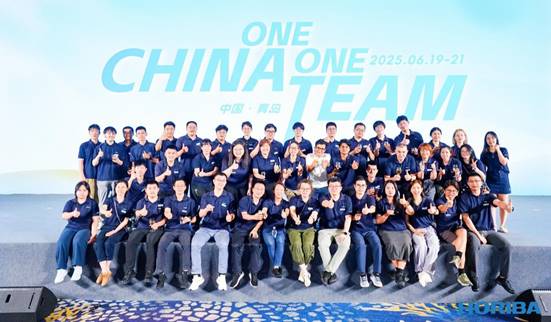
The company actively fostered this spirit of unity through an unforgettable, large-scale team-building event held in Qingdao, operating under the inspiring motto of “One China, One Team.” This was a massive undertaking, bringing together over 600 members from across the entire company, including high-level executives. The core activity involved a coordinated drumming session, where the entire group had to synchronize our individual paces and rhythms to move as one unified entity—a powerful metaphor for our manufacturing and R&D goals. Beyond this, the trip included extensive sightseeing around Qingdao, a relaxing yacht trip, and a lively gala event where I had the exciting opportunity to sing a song on stage for all members. This experience was paramount, not only enhancing my awareness of teamwork under pressure and corporate culture but also fostering deep personal connections that made our professional interactions far more harmonious and collaborative.
HORIBA One China One Team Gala Night

Yacht ride with the Horiba China Team
I received abundant support and guidance that was instrumental to my success. My supervisor , The Manager of the team Mr. Franck Dhalenne from HORIBA, dedicated significant time to introducing me to the project’s technical vision and the team's strategic goals. His mentorship focused on the process methodology of R&D, emphasizing rigorous engineering logic and attention to detail. I also learned a great deal from the core engineers: Gao Xinxing, a senior technical colleague, patiently guided me through the Design intricacies of new equipment setup and debugging the industrial communication protocols. Mr. Zhao from the HR department acted as a constant support, ensuring my adaptation to the new work environment was smooth and stress-free.
The generous assistance and patient tutelage from these mentors were crucial for my professional growth. Their guidance not only accelerated my learning in core areas like embedded systems, industrial communication, and optical-mechanical design but also provided me with important inspiration in terms of professional work attitude and engineering thinking patterns. This internship was not just a process of learning and practice but a significant journey of personal growth, where every day was filled with the tangible accumulation of knowledge relevant to the future of high-tech manufacturing. This invaluable experience, centered around the strategic launch of a new spectrometer product line, will undoubtedly serve as a major driving force and one of the most important starting points in my engineering career.
[It is important to note that as an ongoing R&D project, the final product is not yet launched, and the beta version remains confidential, which cannot be displayed in this article]